Reviewing Gallium Nitride as a Power Semiconductor

The article provides a review of Gallium Nitride power devices, which are considered as potential game-changers in the power electronics industry. It discusses the advantages and challenges of Gallium Nitride power devices.
In power electronic systems, power semiconductors are used as solid-state switches. Silicon (Si), silicon carbide (SiC), and gallium nitride (GaN) are the three power semiconductors that have reached commercialization so far.
Advantages of Gallium Nitride
GaN has better properties than Si and SiC, such as a larger bandgap and a higher critical electric field. High-electron-mobility transistors (HEMTs) can also be built from the AlGaN/GaN heterostructure because it produces highly mobile two-dimensional electron gas (2DEG).
Rapid adoption in power supplies, data centers, Lidar systems, and fast chargers in consumer electronics has led to the recent commercialization of GaN power HEMTs with voltage classes from 15 to 900 V. GaN power devices have allowed for lighter and more efficient power electronics' systems by reducing capacitances and charges.
By 2027, the global market for GaN power devices is expected to grow to over $1.26 billion. GaN power devices are seen as potential game-changers in the aerospace and defense industries, in addition to their increasingly common uses.
Devices used in such settings must be able to withstand harsh conditions, such as high or low temperatures and radiation. As a result, power devices' ability to withstand radiation and extreme temperatures is of extreme significance.
Are Gallium Nitride's Stability and Dependability Guaranteed?
There are still unanswered questions about the stability, reliability, and robustness of GaN devices despite their widespread use. GaN HEMTs are not as widely used as their silicon and silicon carbide counterparts, such as MOSFETs, JFETs, and insulated gate bipolar transistors (IGBTs), because of fundamental differences in architecture and physics. GaN HEMTs are lateral devices that confine their current in a two-dimensional channel only a few nanometers thick, and they lack a p-n junction connecting their source and drain.
Also, unlike Si and SiC devices, which are built on native substrates, many GaN HEMTs are made on silicon and sapphire, which increases the number of defects and traps. Issues with GaN devices' stability, reliability, and robustness are the focus of increasing research and development in both the academic and commercial sectors.
There has also been a rise in the number of papers published about commercially available GaN devices, and there has also been a consistent trend toward publishing reliability studies on the R&D GaN devices demonstrated in research laboratories. This movement coincides with the industry's work to establish GaN qualification standards.
Research devices are often less refined than their commercial counterparts in terms of processing technology, material, and structure, and there are discrepancies between the test conditions used in reliability physics studies and the actual conditions under which a device operates in a practical converter.
In these cases, power electronics engineers have a hard time tying together the physics of reliability with the nonideal behaviors of commercial GaN devices in converters. This difficulty also impedes progress in areas like health monitoring, diagnosis, and protection. Although, in theory, these stability, robustness, and reliability issues are independent of one another, in practice, they often arise together and have fuzzy limits.
Existing Gallium Nitride Devices
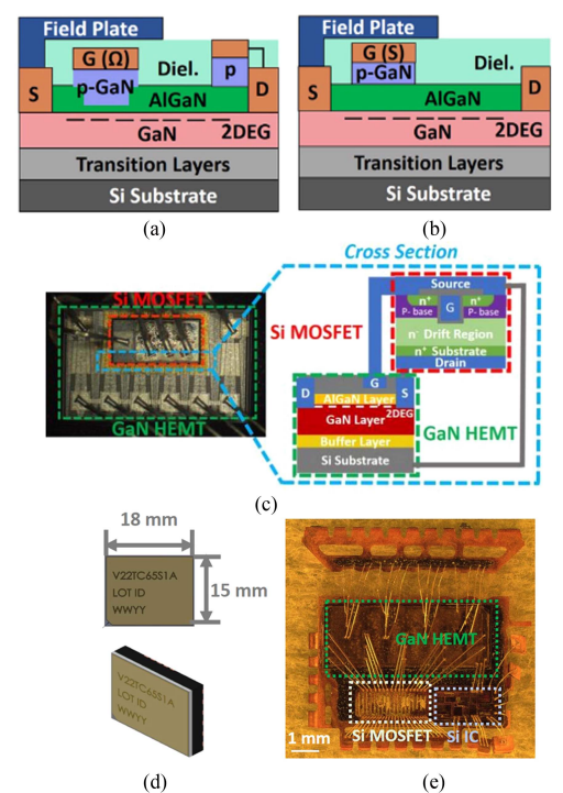
Commercially available GaN products typically use one of four distinct device architectures. The hybrid-drain gate injection transistor (HD-GIT) and the Schottky p-gate high-electron-mobility transistor (SP-HEMT) are two examples.
These technologies are single-component gadgets that enable enhancement-mode (E-mode) operation by incorporating a p-GaN layer into the gate stack. The diagrams for these are in Figs. 1(a) and (b).

Fig. 1. (a) GaN SP-HEMT and (b) GaN HD-GIT (c) Photograph and schematic of a decapsulated cascode GaN HEMT (d) Photograph of a packaged direct-drive GaN HEMT (e) Photograph of a decapsulated direct-drive GaN HEMT from another vendor. Source: IEEE Transactions on Power Electronics
The other two architectures, the cascode structure and direct-drive modules with GaN HEMTs in depletion mode (D-mode), can be thought of as composite devices because they use more than one semiconductor die. A decapsulated cascode HEMT and its schematics are shown in Fig. 1(c). Pictured in Figs. 1(d) and (e) are direct-drive GaN devices and modules from two manufacturers.
Gallium Nitride Device Architecture
The vast majority of available GaN HEMTs on the market today are fabricated on silicon substrates to keep production costs down. The transition layer and the primary GaN buffer layer sit above the substrate. When an AlGaN layer is deposited on top of a GaN buffer layer, the interface between the two materials becomes the primary channel through which electricity flows.
The piezoelectric effect brought on by the lattice mismatch between the two layers results in two-dimensional electro-gyro (2DEG) channels. Above the AlGaN layer, the drain, gate, and source terminals are arranged laterally. The realization of E-mode operation relies heavily on the p-GaN in the gate stack. For most uses in power electronics, the more efficient E-mode operation is ideal.
Types of Gallium Nitride Devices
HD-GIT and SP-HEMT
HD-GIT and SP-HEMT are primarily differentiated at the gate and drain regions. In the HD-GIT, the gate metal makes an Ohmic contact with the p-GaN, while in the SP-HEMT, it makes a Schottky contact. In a typical HD-GIT, the AlGaN layer is recessed, bringing the p-GaN layer closer to the 2DEG.
The AlGaN recess and Ohmic contact on the HD-GIT make it possible to change the conductivity by making it easier to inject holes into the 2DEG channel. To further reduce electron trapping, the HD-GIT's p-GaN region, which is linked to the drain, can inject holes into the channel and buffer. In contrast, the SP-HEMT's channel and buffer regions rely solely on electrons to conduct current, with only a negligible amount of holes being introduced.
Cascode and Direct-drive devices
The conventional high-voltage D-mode GaN devices in the cascode and direct-drive devices are oriented with a lower-voltage E-mode silicon power MOSFET. When the two devices are coupled together, an E-mode device capable of handling high voltage is produced for use in the cascode.
By using an integrated circuit (IC), direct-drive devices take this idea one step further. To improve gate-loop performance and reduce the number of necessary components, a gate driver can be integrated into the power semiconductor. Sensing and protection integrated circuits are included in some devices to provide extra functionality.
These two topologies, in general, allow for the use of D-mode HEMT, which typically has a simpler gate stack than HD-GIT and SP-HEMT. When multiple chips are combined into a single package, however, new failure and instability mechanisms are introduced, which can be triggered and coupled between the chips.
Typical Failure Locations
Due to various stresses from the gate and drain biases, there are known problems with the gate-oxide layer in silicon and silicon carbide MOSFETs. The p-n junction of the MOSFET structure has also demonstrated a number of bipolar stability problems.
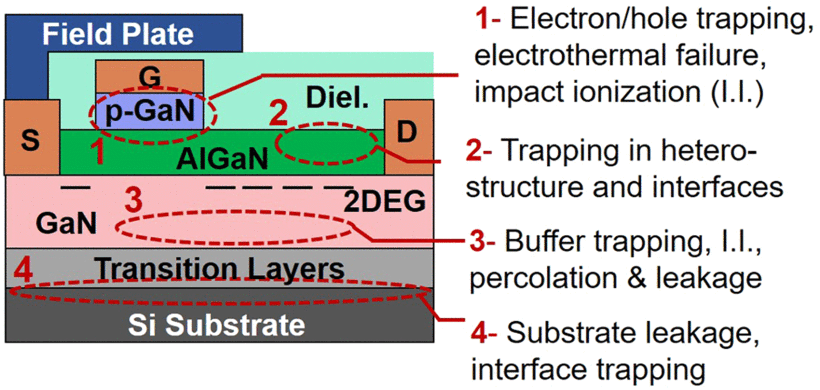
However, as seen in Fig. 2, carrier trapping effects at interfaces and layers within the device are a major contributor to many of the reliability issues that affect GaN HEMTs. Trapping can have a significant impact on the local electric field and current density, which influence the on-resistance, breakdown voltage, and capacitance of the device.
In addition to trapping, device failure can also occur as a result of other physical processes like impact ionization, electrothermal failure, and the formation of percolation paths when subjected to certain stresses.

Fig. 2. Typical trapping locations and other physical processes that can lead to stability, reliability, and robustness issues. Source: IEEE Transactions on Power Electronics
If the carriers created by impact ionization are not effectively removed, for instance, the device could fail destructively. These phenomena typically take place in the GaN HEMT's gate region, AlGaN/dielectric interface, GaN buffer region, transition layers, and silicon substrates. There is a wider variety of potential failure sites in composite-type GaN devices, such as the multi chip interconnect or silicon chips.
Summarizing the Key Points
- Gallium Nitride power devices offer advantages such as reducing capacitances and charges, leading to lighter and more efficient power systems.
- Gallium Nitride high-electron-mobility transistors are lateral devices that confine their current in a two-dimensional channel only a few nanometers thick, and they lack a p-n junction connecting their source and drain.
- The vast majority of available Gallium Nitride high-electron-mobility transistors on the market today are fabricated on silicon substrates to keep production costs down.
- The stability, reliability, and robustness of Gallium Nitride devices are still unanswered questions despite their widespread use and needs further research.
Reference
Kozak, Joseph Peter, Ruizhe Zhang, Matthew Porter, Qihao Song, Jingcun Liu, Bixuan Wang, Rudy Wang, Wataru Saito, and Yuhao Zhang. “Stability, Reliability, and Robustness of GaN Power Devices: A Review.” IEEE Transactions on Power Electronics 38, no. 7 (July 2023): 8442–71.