Printed Circuit Boards Basics
Overview
Among the key theories in electronic equipment is that the printed circuit Board or PCB. It is so basic that we often forget to clarify just what a PCB is. This tutorial aims to breakdown what constitutes a PCB and a few of the common phrases found in the PCB globe.
Over the coming few minutes, we'll discuss the composition of a printed circuit board, structure and composition of a PCB, cover a few language, check out methods of assembly, and talk briefly the design procedure for creating a new PCB.
What Is a Printed Circuit Board (PCB)?
We normally learn about, assess, and sketch electrical boards or electronic circuits using a structure, known as a schematic, that is made up of part symbols connected by lines. The symbols signify everything from fundamental passive components such as resistors or capacitors to sophisticated integrated circuits like microcontrollers, and the traces represent conductive pathways that allow electric current to flow freely from 1 part of the circuit into another.
One thing that all Schematics have in common is the utter inability to drive a motor, or blink an LED or filter out sound, or do some of the other interesting and useful things that we anticipate electric systems to perform. A schematic is also, after all, only a drawing. To really achieve something with a circuit, then we must interpret its schematic into physiological components and physical interconnections. Simple schematics may often be realized to a breadboard, but the huge majority of circuit designs become a reality physically on a printed circuit board, or PCB for short.
Understanding PCB terminology
- PCB - Printed Circuit Board
- Trace - A conductive interconnection
- Pads - Connection points for components pins that rest on board
- Through-holes - Connection points for components pins that are inserted on the holes on the board
- Vias - small conductive holes for signal transfer or voltage supply
- Mounting holes - mechanical mounting function
- Plating - conductive material deposited on the interior of a drilled hole
- Annular ring - width of copper remaining in a through-hole
- Copper pour - is the conductive material
- Plane - a single large copper pour
- Silk screen - also called reference designator offers supplemental information on pcb
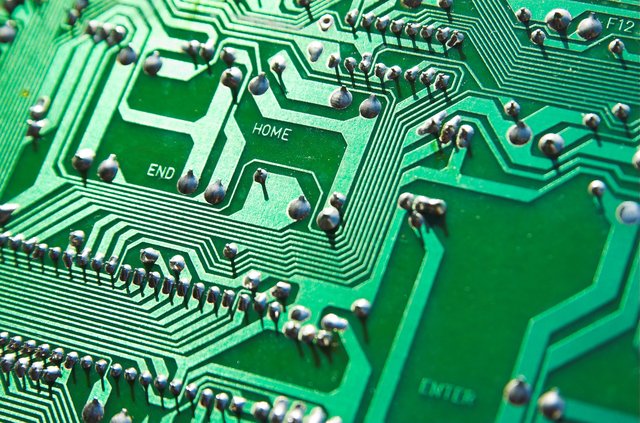
The Fundamental Structure of a PCB
Based on research and input from our engineering colleagues we know that the very basic printed Circuit board is a flat, rigid, insulation material which has thin conductive structures sticking to a single side. These conductive structures create geometric patterns consisting of, by way of instance, rectangles, circles, and squares. You can, clearly see long, thin rectangles interconnections which are equivalent of wires, and various shapes do serve as connection points for elements. You can see flexible PCB boards below:
A single-layer PCB is extremely prohibitive; the circuit realisation won't make efficient use of available place, and also the engineering designer may have difficulty creating the necessary interconnections.
Incorporating additional conductive layers makes the PCB more streamlined and easier to design. As you do more project with PCB you will realise that a four layer board has far more benefits as it consists of the upper coating(top), the underside layer(base), and 2 internal layers. Anyway, a two-layer board is a significant improvement on a single-layer plank, and most programs benefit from having at least four layers. A four-layer board are nonetheless the official designations on the planet of PCB layout and fabrication.)
Stackups
What is a Stackup?
The stackup is your arrangement of conductive and insulating layers in a multilayer PCB. When doing project (personal engineering builds), we recommend using a four-layer structure whenever possible. This is mainly because a four-layer board enables you to devote one inner layer to ground and the other internal layer to power-supply voltages. This stackup arrangement facilitates PCB layout and also helps you to attain enhanced circuit operation for maximum benefit.
PCB composition explained
In the introduction, we defined what a PCB is and in this section we will explain the layers that makeup a PCB which you will realise its layered up like a cake - with alternating layers of various materials that are laminated into one objectlike thing of technological beauty.
Let's start in the core of a PCB and work outwards to what you see as a shell:
FR4
The foundation material, is normally fiberglass. Over the year, the most frequent designator for this fiberglass would be"FR4". This solid core gives the PCB its own rigidity and mass. You will find other PCB's constructed from flexible high-temperature plastic like Kapton.
If your a novice in PCBs; you will have realised they there are a choice of thickness depending on which brand you go for you can have anything from 0.8mm - 1.6mm thick board. Some of the popular board manufacturers include "" which you can see here.
Depending on your budget, you will find Cheaper PCBs that are made from materials such as epoxies / phenolics which lack the durability of FR4 and also tend to have a very distictive poor odour when you soldering and you will find them mainly non invasive consumer electronic equipment.
Copper
On top of FR4 comes a thin layer is of copper foil, which can be laminated into the Board with heat and glue. In lower price digital gadgets the PCB may have copper on just 1 side, however, on double sided PCBs, copper can be applied to both sides of this FR4 substrate. When you hear engineers refering to double sided or 2-layer board they are referring to the amount of copper layers i.e. two layers. In general, you can have upto 16 layers even more. The copper thickness which is specified in weight depends on the power they need to manage and it would usually be 1 Ounce per foot and more thickness depending on the demand.
Soldermask
This layer goes on top of the copper foil. The soldermask coating provides the PCB its green colour but you will see other manufacturers with different colour boards including red and white. This layer acts as an insulation and precaution so that the copper traces don't accidental get into contact with other metal, solder, or conductive pieces. As a result, it enables the consumer/engineer to solder into the appropriate places and prevent solder jumpers.
Silkscreen
The silkscreen is usually a white coating that is applied on top of the soldermask layer and generally works as a naming convection with letters, numbers, and symbols on the PCB. These indicators allow individuals and engineers implement rapid assembly as they allow them better understand the board.
Although you can use other silkscreen colours, it is uncommon to see over one colour on a single plank. Best practice is to use one silkscreen colour all through.
This section explains physical structures located on PCBs and gives you the words that we use to spot them.
Designing your own Printed Circuit Board
The the Inner workings of PCB Design are way too in depth to get into here, but in the event that you really want to get started, below are a few pointers:
You can download the Hitchhiker's Guide to PCB Design free ebook here:
 The Hitchhiker's Guide to PCB Design
How can you go about designing your PCB?
- Find a CAD package like OrCAD:
- There are a good deal of low-cost or completely free options out there on the market for PCB design. However, we would advice looking for one that offers bundle packages for those doing this as a profession. Things to look at when picking a bundle:
-
- Community support: The more people using this, the more likely you should come across ready-made libraries with the components you want.
- Ease-of-use: When it's painful to use it, then you won't ever.
- Robust capability: You want an applications that doesn't place limitations on your design layouts and you can scale it when you need to.
- Portability: You also want to be able to export or convert design and therefore, check that you are not limited on one product just incase you need to migrate and work on another suppliers to improve on your design. Check out OrCAD PCB Design software
- Look at other people's designs to see what they've done. Open Source Hardware makes this easier than ever to build and improve on others know-hows.
- Practice makes perfect. Nearly every product designed to perfection has been created out of the experience of years of experience and practice from engineers, therefore, practice and practice again.
- Maintain low expectations. Your first board design will have plenty of issues. However, same as bullet #3 you improve on every design.
- Schematics planning is important. Attempting to design a pcb with no good schematic in place first might be futile leading to time wastage.
To browse through our distributors & manufacturers PCB panels inventory, click here and enter your MPN, otherwise, see one PCBs & Breadboards example below: