Analog Devices’ LTM2887 – If a Digital Bus Needs Galvanic Isolation
In theory, digital buses are intended to connect things to one another. Sadly, one sometimes wants but a logical connection – in many cases, galvanic isolation helps out. Should you ever feel like isolating very fast buses, definitely give the LTM2887 a chance.
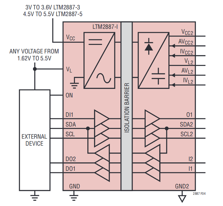
From a technical point of view, Linear Technologies attempt at entering the galvanic isolator IC fray is relatively simple. Figure one tells us that the LTM2887 has a total of three transcievers for one direction, which can be used to route arbitrary signals across the isolation border at the middle. It provides for an isolation voltage of up to 2500Vdc.

Adding galvanic isolation to an SPI bus could not be easier
Linear Technologies experience in the degree of sensor design shows itself in the adding of a two-output power supply which can provide small amounts of energy (100mA at 5V per channel) across the isolation border. This measure is useful in that it lets you power small bits of electronics without needing an additional transformer wiring or a similar galvanic isolator. One of the two output channels can furthermore be regulated, removing the need for an additional voltage regulator inside of the “isolation island”.
I2C’s open drain architecture has always had the dubious distinction of making a galvanic isolator designers life interesting. The LTM2887 works around this problem via the design trick shown in figure two – one of the transcievers is provided with a feedback path, thereby allowing the two sides of the circuit to interact with one another. This pair of pins can then be used to route the SDA pin – as clock generation is the master’s sole responsibility in most I2C buses, SCL can simply run from master to slave.
From a space point of view, deploying the (somewhat pricey) part is not too difficult – the 15mm × 11.25mm × 3.42mm BGA housing should fit even the tightest of PCBs. Sadly, hand-soldering the LTM2887 is not really possible due to the BGA housing.